

The magic of ASML and the startups looking to disrupt them

ASML builds the machines that enable the world’s most advanced chips. The Dutch company based in Veldhoven reported €28bn in net sales in 2024, driven primarily by its unique lithography systems, which enable leading-edge logic and memory.
ASML’s extreme ultraviolet (EUV) systems use a reflective mask (reticle) to pattern wafers for the world’s leading-edge semiconductors. They do so through a mind-bendingly complex process that integrates optics, laser-produced plasma, vacuums, sub-nanometer robotic steppers, metrology, inspection and simulation.
ASML’s EUV systems generate 13.5 nm light by firing a high-power laser at 50,000 tin droplets per second. That light is collected and reflected through ultra-precise mirrors in high vacuum, while sub-nanometer stages align and scan the wafer. With the pattern encoded in the light, the system’s optics shrink and focus the pattern onto a photosensitive silicon wafer.

ASML acts as a system integrator, working closely with over 5,000+ suppliers on shared roadmaps to push the frontier. These include Zeiss, TRUMPF, and imec, which are producing subsystems at the bleeding edge of optics, lasers, metrology, etc. They own Cymer for EUV light sources and are large shareholders of Carl Zeiss SMT for optics. ASML spends an average of 15% of bookings per annum on R&D, which in 2024 amounted to €4.3bn.
ASML ships a whole system, the scanner, the installation, the control loop and the maintenance. ASML’s latest generation, the High-NA EUV scanner, is roughly the size of a bus, and targets 8 nm single-exposure resolution with 185 wafers/hour throughput for high-volume manufacturing. It costs €350m a pop, weighs 165 tons, is shipped with up to 30 sea freight containers and installed and calibrated at customer sites by a team of ASML engineers.
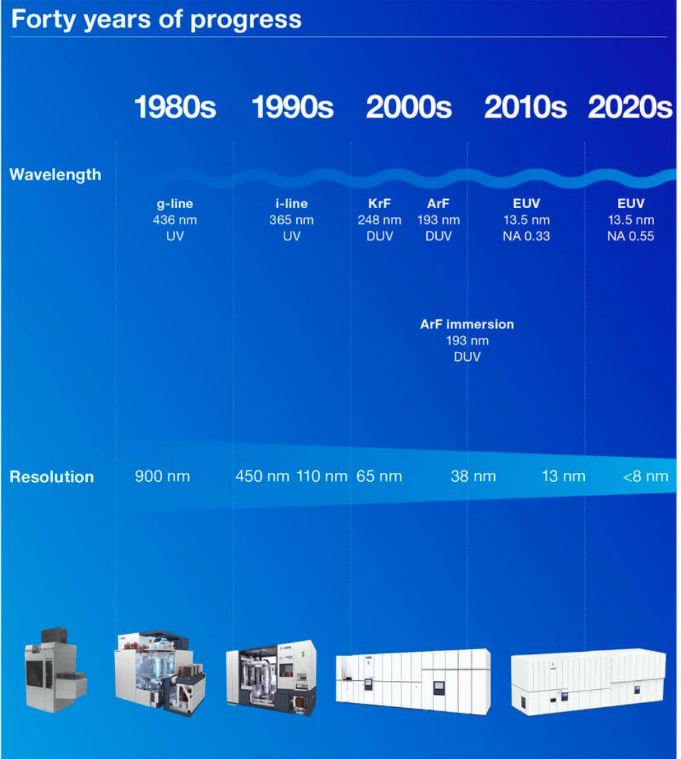
Over the last 30 years, ASML has been following the trajectory of Moore’s Law, building tooling for ever smaller and denser semiconductor fabrication. The company is the sole supplier of EUV scanners to leading fabs, TSMC, Samsung and Intel. TSMC, based in Taiwan, is the leader in fabrication of advanced semiconductors, namely sub 5nm chips needed for frontier AI training and inference. TSMC produces chips for NVIDIA, Apple, and Tesla, among others. It is a source of global tension, particularly with China, because its dominance in advanced chips confers strategic advantages to its customers and their host nations. ASML is the chokepoint of chokepoints, a seemingly irreplaceable tool in the creation of frontier AI.
Beyond Moore’s Law
However, change is afoot. As Moore’s Law slows and in turn chip transistors shrink, scaling chip production is having to evolve along a few new tracks. One lane keeps shrinking transistors (EUV → High-NA, backside power, new device types), while the other stitches more silicon together (chiplets/UCIe, advanced packaging, optical I/O), reducing how often you need another EUV pass.
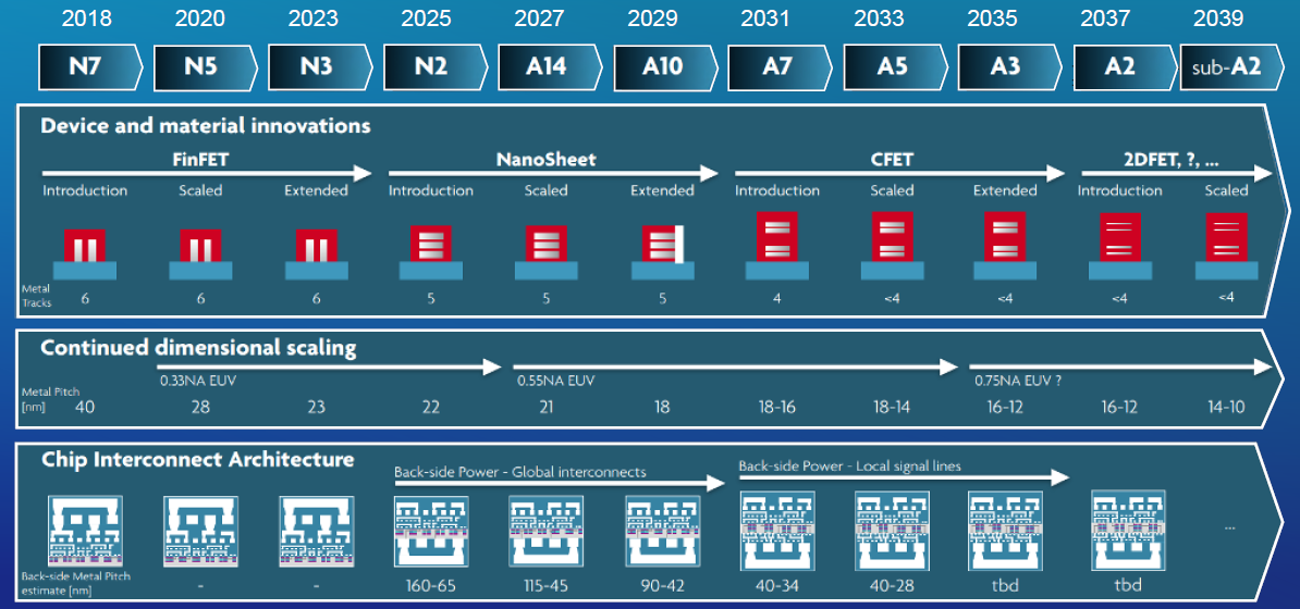
TSMC says A16 (1.6 nm) won’t require ASML’s new High-NA EUV tools, it will stick with today’s 0.33-NA EUV plus process innovations and backside power, adopting High-NA EUV only if and when the economics make sense. Intel, by contrast, plans to use High-NA for 14A (1.4 nm) if it can find a customer. The practical breakpoint is when one High-NA exposure is cheaper and cleaner than multi-patterning on today’s EUV.
Meanwhile, a wave of new tooling and fabrication is rising to reduce reliance on more EUV passes or to extend silicon computation ‘beyond Moore’ (chiplets/UCIe + hybrid bonding, advanced packaging like CoWoS), rerouting performance into photonics (co-packaged optical I/O), or challenge lithography itself (NIL “stamping”, novel high-brightness sources), with backside power and CNT devices changing what must be patterned in the first place.
mo’ EUV, mo’ problems
Most new startups are attempting to stitch more silicon together. Silicon photonics replaces copper with light and pushes performance through foundry photonics modules and optical assembly rather than EUV layers. One such company is Lightmatter, now mass-producing its Passage photonic interposer with semi fab GlobalFoundries, and pairing that with a photonic chiplet to wire AI clusters at terabit scale. They are using photonics plus advanced packaging and optical alignment to generate performance. Celestial AI is pursuing a similar idea with its “Photonic Fabric,” an optical fabric between compute and HBM. The manufacturing emphasis is on silicon photonics device layers and co-packaged assembly rather than lithography escalations. Ayar Labs is taking in-package optical I/O right into real designs via a long-running GlobalFoundries photonics process (45CLO/Fotonix lineage) and a partnership with Alchip, an explicit bet that co-packaged optics becomes standard kit for hyperscalers. Avicena goes variant with microLED-based optical links that can be manufactured in the microLED ecosystem and coupled to silicon, again a fabrication path that scales mostly with assembly and photonics steps, not more exposure passes.
Let there be light
Other startups are targeting EUV’s light source, one of the more fragile subsystems with the etching process. One such company is Inversion Semiconductor, whose compact particle-accelerator light source intends to be tunable and significantly brighter. Its ambition is to drive faster scanners or even shorter wavelengths. It’s very early-stage physics-and-laser engineering, but if it worked, it would shift EUV economics from the source outward.
Breaking the pattern
Some teams are changing what needs patterning in the first place. Backside power delivery moves power rails to the silicon wafer’s backside using bonding, thinning, and backside metal. Freeing front-side area and easing routing congestion without adding an EUV-heavy front-end step explosion. That’s mainly a foundry game. On the materials side, Chiral Nano is building robotic wafer-scale assembly machines that place carbon-nanotube devices at speed, plus a foundry service for customers who want CNT devices without touching the chemistry. The short-term commercial wins are likely in RF/analogue and sensing; the tooling bet is that wafer-scale, repeatable assembly unlocks useful device classes before general-purpose CNT logic arrives.
Absolutely Fab(olous)
Then there are the teams that want to reinvent the fab itself. Atomic Semi (Jim Keller and Sam Zeloof) is building a small, fast fab by making its own tools and iterating quickly. They are using e-beam and compact toolchains for speciality devices and fast prototyping rather than a head-to-head fight with EUV logic. If they compress time-to-silicon for new ideas and lagging nodes, some budgets that would have gone to litho-intensive mask sets move to agile, lower-capex flows. Atum Works is attempting to build a 3D nanolithography platform that prints multi-material structures with 100 nm features at wafer scale. The manufacturing recipe uses advanced photo polymerisation and precise optics to write 3D geometries. It’s not a replacement for 2D logic lithography today, but it is a plausible production path for 3D interposers, photonic structures, sensors, and packaging features that are awkward or impossible to realise with planar stacks.
Possible Future
On a 5-10 year view, ASML will be displaced, its far too complex and embedded. Photonics and chiplet packaging move performance into foundry/OSAT assembly and optical toolchains. CNT assembly and 3D nanoprinting try to grow entirely new device classes whose manufacturing scales with robots and optics rather than exposures. Each path has rough edges but they all share the same strategic intent, to reduce how often we have to pay for another EUV pass.
❤️ If you enjoyed this piece, please like and share it with your smartest friend